
Executive Programme in Semiconductor Manufacturing and Technology (Batch 2)
Features
Programme Overview
Step into the future of innovation with IIT Delhi’s 6-month Executive Programme in Semiconductor Manufacturing & Technology, designed exclusively for working professionals. Gain cutting-edge expertise in semiconductor processes, design, and fabrication, while enhancing your skills to thrive in this rapidly evolving industry. Delivered by industry experts and academic leaders, this programme combines flexibility with rigor, empowering you to upskill without pausing your career.
₹ 1,25,000 + 18 % GST
Registration Closed
Class Schedule
Class Timing: Sundays 9:30 am - 12:30 pm
Eligibility Criteria
B.Tech/M.Sc./10+2+3 diploma holders.
Programme Highlights
E-Certificate Of Successful Completion From CEP, IIT Delhi: Participants Must Attend At Least 40 % Of The Lectures And Tutorials. Those Who Secure More Than 50% Of The Assessment Marks Along With The Required Attendance Will Receive An E-Certificate Of Completion. Meanwhile, Participants Who Meet The Attendance Requirement But Score Less Than 50% In Assessments Will Be Awarded An E-Certificate Of Participation.
Expert-Led Curriculum: Delivered By Faculty From IIT Delhi’s Optics & Photonics Center, Complemented By Guest Lectures From Industry Leaders.
Real-World Relevance: Gain Hands-on Insights Into Semiconductor Manufacturing Processes, Emerging Technologies, And The Latest Industry Trends.
Prestige: Certification From One Of India’s Most Renowned Institutions, Boosting Your Professional Credentials.
Immersive Experience: An Optional Two-day Campus Immersion At IIT Delhi For In-depth Interactions And Networking Opportunities.
Programme Modules
Semiconductor Materials | Understand the basic properties of intrinsic and extrinsic semiconductors, including concepts like doping and charge carriers. |
Energy Band Theory | Explore energy bands and how they differentiate semiconductors from conductors and insulators. |
P-N Junctions | Learn about the formation of p-n junctions and their role in basic semiconductor devices like diodes. |
Basic Semiconductor Devices | Get an overview of simple devices such as diodes and transistors, focusing on their design and functionality. |
Semiconductor Applications | Discuss real-world applications of semiconductors, from simple electronics to more advanced systems like LEDs and solar cells. |
Introduction to Semiconductor Fabrication | Gain insights into the semiconductor manufacturing process. Understand the importance of precision in fabrication. |
Lithography Techniques in Fabrication | Explore the various lithography methods used in semiconductor production. Learn how these techniques impact device resolution and performance. |
Doping and Material Modification | Understand the principles of doping and its effects on semiconductor properties. Examine methods for modifying material characteristics. |
Etching Processes in Semiconductor Manufacturing | Study the etching techniques essential for device fabrication. Learn the differences between wet and dry etching methods. |
Cleanroom Practices and Environmental Control | Delve into the importance of cleanroom environments. Understand the protocols and technologies used to maintain cleanliness in semiconductor fabs. |
Carrier Transport Mechanisms | Examine drift, diffusion, and recombination processes and their impact on device operation. |
Junction Behavior | Analyze the behavior of p-n junctions, including electric fields, depletion regions, and forward/reverse bias conditions. |
Scaling and Miniaturization | Understand the effects of device scaling on performance and efficiency, particularly in modern transistors. |
Material Selection | Explore the role of different semiconductor materials (e.g., silicon, gallium nitride) in optimizing device performance. |
Thermal and Power Management | Learn strategies to manage heat and power in high-performance semiconductor devices for improved reliability. |
Semiconductors in Electric Vehicles | Explore how semiconductors are transforming the electric vehicle industry. Understand their role in power management and control systems. |
Data Centers and High-Performance Computing | Delve into the impact of semiconductor technology on data centers. Learn about energy efficiency and processing capabilities. |
Semiconductors in Space Applications | Study the unique challenges of semiconductor use in space. Explore materials and technologies designed for extreme environments. |
Artificial Intelligence and Machine Learning | Examine how semiconductors enable advancements in AI. Learn about specialized chips for neural networks and deep learning. |
Entertainment Technologies: Gaming and Beyond | Explore the role of semiconductors in the entertainment industry. Understand their applications in gaming, VR, and media streaming. |
Global Semiconductor Market Overview | Understand the structure and size of the global semiconductor market, including major players, key regions, and market segments. |
Supply Chain Dynamics and Challenges | Explore the semiconductor supply chain, including raw material sourcing, manufacturing processes, and recent disruptions like the global chip shortage. |
Emerging Technologies and Growth Opportunities | Identify new trends in semiconductor technology, such as AI, 5G, and automotive applications, and explore potential commercial opportunities. |
Geopolitics and Semiconductor Trade Policies | Analyze the impact of geopolitical factors on the semiconductor industry, including trade wars, export controls, and government policies. |
Investment and Innovation in Semiconductor Startups | Learn about venture capital, funding strategies, and the role of innovation in driving growth within the semiconductor ecosystem. |
Learning Outcomes
Return on Investment: Master semiconductor devices and technologies, from basic concepts to advanced applications in EVs, AI, space, and more. Gain the skills to lead and innovate in this rapidly evolving industry.
Accelerate Your Professional Growth: Learn to design and fabricate cutting-edge semiconductor devices. Position yourself as an expert in emerging technologies like AI and automotive.
Explore the Opportunities of the Semiconductor Revolution: Stay ahead of the semiconductor revolution by understanding market trends and commercial opportunities. Unlock new pathways for innovation and success.
Empower Your Organization: Leverage insights into global market dynamics and lead your organization in semiconductor technology. Drive growth and capitalize on next-gen advancements.
Empower Your Organization: Leverage insights into global market dynamics and lead your organization in semiconductor technology. Drive growth and capitalize on next-gen advancements.
Programme Coordinator

Professor Awanish Pandey
Assistant Professor
Optics and Photonics Centre
Indian Institute of Technology
Prof. Awanish Pandey is an Assistant Professor at the Optics and Photonics Centre, IIT Delhi. He has nearly a decade of experience in semiconductor technology, having worked with leading semiconductor foundries like imec, Belgium, and renowned research facilities such as CERN in Geneva, Switzerland. He obtained his Ph.D. from the Indian Institute of Science, Bangalore, in 2019. Primarily, his research revolves around manipulating the flow of photons in nanophotonic structures made of semiconductors such as Silicon. Currently, his research group is focusing on developing ultra-high-speed integrated photonic links and systems for 6G communication. Additionally, he plays a key role in the National Quantum Mission (NQM), contributing to the development of India’s first photonic quantum processor.

Professor Dheeraj Pratap
Assistant Professor
Optics and Photonics Centre
Indian Institute of Technology
Dheeraj Pratap is an Assistant Professor at the Optics and Photonics Centre (OPC) of the Indian Institute of Technology (IIT) Delhi. He obtained his PhD degree in metamaterials from the IIT Kanpur in 2016. Later, he was a postdoctoral researcher in GRESPI at the University of Reims Champagne-Ardenne, France. For a short time, he worked as a project scientist at the IIT Kanpur and then as an Assistant Professor at the Veermata Jijabai Technological Institute (VJTI) Mumbai. Before joining the OPC, he was a CSIR-Nehru Science Postdoctoral Fellow at the CSIR-Central Scienti c Instruments Organization (CSIO) in Chandigarh. His research interests include photonic metamaterials, metasurfaces, plasmonics, and photothermal effects. He has published several research articles in national and international journals of repute and has a few patents.
Programme Sample Certificate
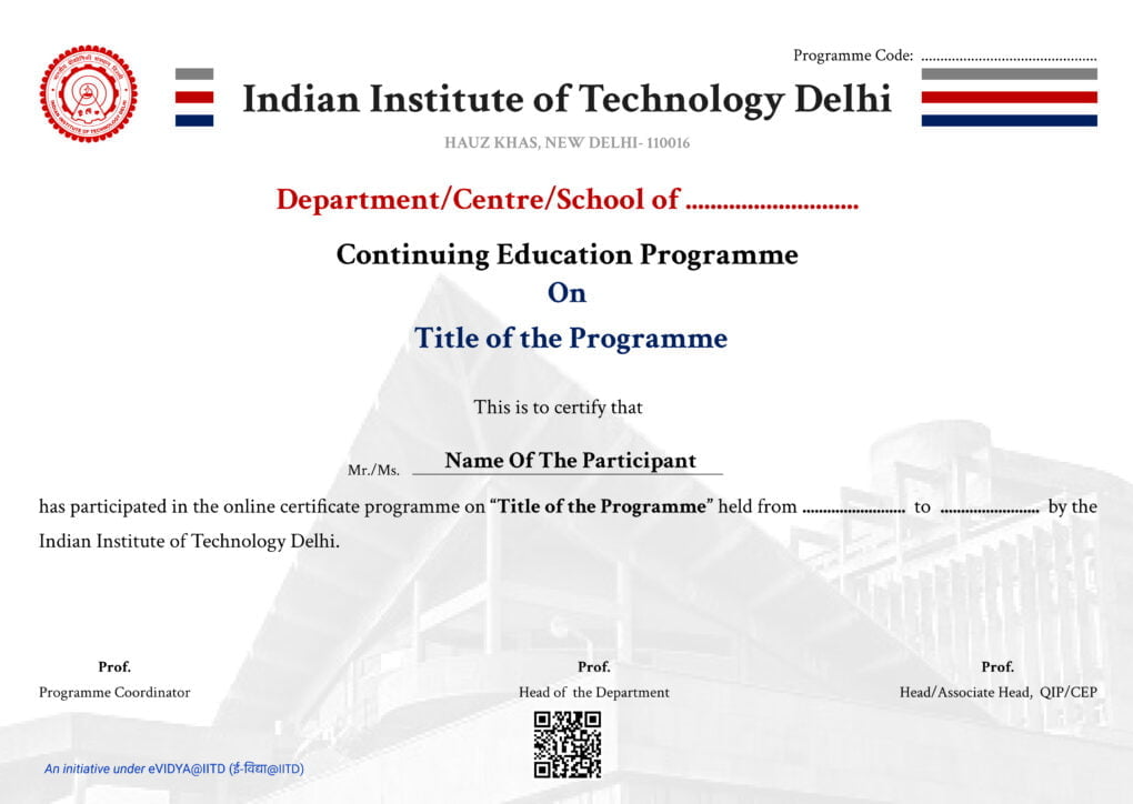
Participation Certificate Awarded with at least 40% attendance and below 50% marks.
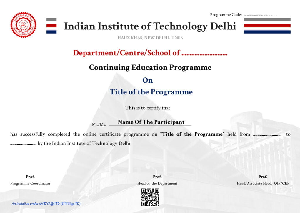
Successful Completion Certificate Awarded with a minimum of 40% attendance and over 50% marks.
The above e-certificate is for illustrative purposes only, and the format of the e-certificate may be changed at the discretion of IIT Delhi.
Only an e-certificate will be provided, and it will be issued by CEP, IIT Delhi.
The organizing department of this programme is the Optics & Photonics Center, IIT Delhi.
Installment Schedule
Programme Fee INR 1,25,000 + GST
Installment | Installment Date | Amount (₹)* |
I | Within 3 days of offer rollout | ₹ 60,000+GST |
II | On or before 25th January, 2026 | ₹ 65,000+GST |
Note:
GST @ 18% will be charged extra in addition to the fee
All fees should be submitted in the IITD CEP account only, and the details will be shared post-selection.
The receipt will be issued by the IIT Delhi CEP account for your records
Refund Policy
Candidates can withdraw within 15 days from the programme start date. A total of 80% of the total fee received will be refunded. However, the applicable tax amount paid will not be refunded on the paid amount.
Candidates withdrawing after 15 days from the start of the programme session will not be eligible for any refund
If you wish to withdraw from the programme, you must email cepaccounts@admin.iitd.ac.in and cepdelhi@digivarsity.com, stating your intent to withdraw. The refund, if applicable, will be processed within 30 working days from the date of receiving the withdrawal request.
Frequently asked questions
This 6-month programme equips professionals with a strong foundation in semiconductor devices, fabrication processes, and advanced applications, delivered through live online sessions and an optional campus immersion at IIT Delhi.
It is designed for engineers, technologists, and professionals from electronics, semiconductors, nanotechnology, and related fields who want to enhance their expertise or transition into the growing semiconductor industry.
Participants are assessed through quizzes, assignments, and module-based evaluations designed to test both conceptual clarity and problem-solving skills relevant to semiconductor technology. All assessments are conducted online with proctoring to ensure fairness and academic integrity.
Yes. Participants will interact with IIT Delhi faculty, peers, and industry experts during live sessions, with further opportunities to connect during the optional 2-day campus immersion.
Participants who meet the evaluation requirements will be awarded an e-Certificate of Successful Completion from CEP, IIT Delhi. Those who fulfill the minimum attendance but not the evaluation criteria will receive a Certificate of Participation. This certificate validates your expertise and commitment to semiconductor manufacturing and technology, enhancing your professional profile.