
Certificate Programme in Digital VLSI Design
Features
Programme Overview
The demand for digital VLSI design services is intricately linked to the overall expansion of the semiconductor industry. With projections indicating that the global semiconductor industry could reach a trillion-dollar valuation by 2030, there is a growing imperative to create efficient and specialized Digital Integrated Circuits. This advanced certification course in Digital VLSI Design aims to enhance participants’ proficiency in crafting digital integrated circuits, encompassing areas such as RTL (Register Transfer Level) design, synthesis, verification, and testing. Additionally, it provides hands-on exposure to industry-standard tools and design methodologies employed in digital VLSI design, including CAD tools, hardware description languages (HDLs), and simulation tools. Faculty members at the Centre for Applied Research in Electronics (CARE) at IIT Delhi equip participants with the requisite skills and knowledge to pursue career opportunities in digital VLSI design across semiconductor companies, electronics design firms, or research institutions. Moreover, this program fosters participants’ problem-solving capabilities by immersing them in practical design projects and case studies, empowering them to address intricate design challenges with efficacy.
Registration Closed
Class Schedule
Duration: 6 Months
Session Timings: Sunday from 10:00 AM to 1:00 PM
Eligibility Criteria
Any Electronics, Electrical, Physics, or Computer Science Graduate.
Candidates pursuing a graduation degree are also eligible; however, preference will be given to applicants with experience.
Diploma holders (10 + 3) or (10 + 2 + 3) are also eligible.
Programme Highlights
Certification From CEP, IIT Delhi
Learn From Top Faculty In VLSI Design
3 Days Campus Immersion
Real-world Case Studies
Industries Visits/Interactions With The Leaders
Networking Opportunities During Campus Immersion
Programme Modules
CMOS ASIC Design Flow
The MOSFET Device
The Interconnects
The CMOS Inverter
Inverter Delays and Power Dissipation
The Combinational Logic Gates
The Sequential Logic Gates
Circuit Simulations using LTspice
Digital Circuit Design Example
Low-Power CMOS Circuit Design
RTL Design using Verilog HDL
RTL Verification and Finite State Machines (FSM)
Capstone Project in Verilog Design & Synthesis
Floor-Plan
Placement
Static Timing Analysis
Clock Tree Synthesis and Signal Integrity
Routing and DRC
Layout Parasitic Extraction
Advanced Floor planning and Placement Strategies
Clock Tree Synthesis and Advanced Timing Analysis
Signal Integrity and Electromigration Challenges
Hardware architectures for AI/ML
Neural network accelerator design
Tensor processing unit fundamentals
Hardware-software co-design for AI applications
Optimization techniques for ML hardware
Edge computing architectures
Security hardware implementation
AI based VLSI Design (CAD)
Post Silicon Chip Validation
Chip Integration and Packaging
Introduction to 3D IC Design and Chiplet Architectures
Automotive IC design considerations
IoT chip design
5G/6G communication hardware
UNIX Environment
Basic Linux Commands
Shell-Scripting
Introduction to PERL Programming
PERL Programming
Argument Parsing, Loops and Functions
File Handling
Regular Expressions in PERL
24 hours of Lab module is planned in the programme.
Labs will be conducted online. Various projects and hands-on training will be provided during lab hours.
Circuit Simulation Tool: LTSpice
Verilog Simulation Tool: ModelSim
FPGA/RTL Design Tool: Xilinx Vivaldo
FPGA Development Tool: Quartus Prime Lite
Operating System and Languages: Linux/Tcl
Some of the projects planned are given below:
Project 1: Combinational and Sequential CMOS Circuit Design
Project 2: CMOS Low Power I/O Circuit Design
Project 3: Power Management IC (PMIC) Design
Project 4: Clock Tree Synthesis and Static Timing Analysis
Project 5: Design for Test (DFT) and Automatic Test Pattern Generation (ATPG)
Learning Outcomes
Demonstrate a solid understanding of design principles, including logic synthesis, timing analysis, and physical design.
Utilize industry-standard VLSI design software to design, simulate, and verify digital integrated circuits.
Apply advanced VLSI design techniques such as low-power design, high-speed design, and design for testability (DFT).
Analyze and optimize the performance, area, and power consumption of digital VLSI designs.
Work effectively in interdisciplinary teams to tackle real-world VLSI design challenges and projects.
Tools
Figma
Canva
Programme Coordinator
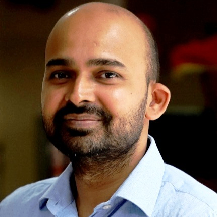
Prof. Ankur Gupta
Associate Professor
Centre for Applied Research in Electronics
Indian Institute of Technology Delhi
Dr. Ankur Gupta is an associate professor in the Centre for Applied Research in Electronics (CARE) at IIT Delhi. He is also a core member of the VLSI Design Tools and Technology (VDTT) program offered jointly with the Electrical Engineering and Computer Science department. He holds a master's degree in VLSI & Embedded Systems and a Ph.D. Degree in Microelectronics. He has more than 12 years of experience in VLSI and Microelectronics. He also has more than 6 years of Industrial experience with the world's top MNCs, i.e., Intel Inc., Texas Instruments, and Global Foundries.
Programme Sample Certificate
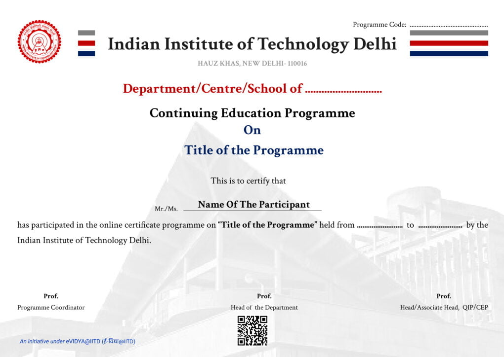
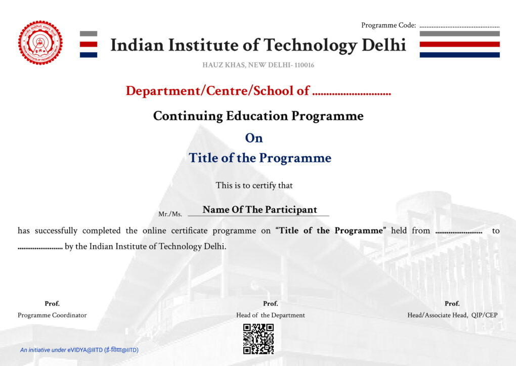
Candidates who score at least 50% marks overall and have a minimum attendance of 50% will receive a ‘Certificate of Completion’ from CEP, IIT Delhi.
Participants who are unable to score 50% marks in the evaluation but maintain a minimum attendance of 50% will be eligible for the ‘Participation Certificate’ from CEP, IIT Delhi.
he above e-certificate is for illustrative purposes only, and the format of the certificate may be changed at the discretion of IIT Delhi.
Only an e-certificate will be provided, and it will be issued by CEP, IIT Delhi.
The organizing department of this programme is the Centre for Applied Research in Electronics (CARE) at IIT Delhi.
Installment Schedule
Programme Fee: 1,20,000 +GST
Installment | Date | Amount |
1st Installment | 3 days from the date of the offer | 80,000 |
2nd Installment | 04th October 2024 | 40,000 |
Note:
*GST @ 18% will be charged extra in addition to the fees.
Refund Policy
Candidates can withdraw within 15 days of the programme start date. A total of 80% of the total fee received will be refunded. However, the applicable tax amount paid will not be refunded on the paid amount. • Candidates withdrawing after 15 days from the start of the programme session will not be eligible for any refund.
If you wish to withdraw from the programme, you must email cepaccounts@admin.iitd.ac.in and crm.supportiitd@jaro.in, stating your intent to withdraw. The refund, if applicable, will be processed within 30 working days from the date of receiving the withdrawal request.
Frequently asked questions
This programme in Digital VLSI Design offers hands-on exposure to industry-standard tools and methodologies, along with practical design projects and case studies, which enhance problem-solving capabilities and readiness to tackle real-world design challenges.
Participants will gain exposure to industry-standard tools such as CAD tools, hardware description languages (HDLs), simulation tools, and scripting languages like Shell, Tcl, Perl, and Python. They will also learn about design synthesis, DFT, scan, ATPG, and other essential methodologies in digital VLSI design.
The lab module consists of 24 hours of online sessions where participants engage in hands-on projects and training related to digital VLSI design. Various projects, including Combinational and Sequential CMOS Circuit Design, Power Management IC Design, and Clock Tree Synthesis, are planned to provide practical experience.
Following are some of the ideal career prospects
Digital VLSI Design Engineers: Participants can embark on careers involving the design and development of digital integrated circuits, focusing on optimizing performance and efficiency.
ASIC Designers: Learners can pursue roles specializing in Application-Specific Integrated Circuit (ASIC) design, tailoring circuits to specific applications or functionalities.
Verification Engineers: Opportunities exist in verification engineering, where participants ensure the functionality and correctness of digital designs through rigorous testing and validation processes.
Academic Research: Those inclined towards academia can engage in further research in digital VLSI design, contributing to advancements in the field through innovative research projects and publications.
Potential career paths include VLSI Designer, VLSI Test Engineer, Digital System Analyst, and IC Verification Engineer. The job market for individuals with Digital VLSI Design skills is promising, with increasing demand due to technology advancements. Moreover, opportunities in academia, research, and development are also available for experts in this field.
The total programme fee is INR 1,20,000/- + GST. Interested individuals are encouraged to connect with Jaro Education’s admission experts for more information on the enrollment procedure.