
Certificate Programme in Digital VLSI Design ( Batch 2)
Features
Programme Overview
The VLSI (Very Large Scale Integration) industry sits at the core of modern electronics. From smartphones and laptops to electric vehicles, 5G networks, and AI-driven systems, every advanced technology today is powered by chips designed using VLSI.
As global industries accelerate toward AI, IoT, automation, and high-performance computing, the demand for compact, efficient, and reliable semiconductor designs continues to rise.
India’s Growth Story
India is fast becoming a global semiconductor design hub.
Nearly 20% of the world’s chip design engineers are based in India
Major global semiconductor companies run large R&D and design centers across the country
₹ 1,35,000 + 18 % GST
Registration Closed
Class Schedule
Live Online | Time : 10 AM to 01 PM, Every Sunday
Eligibility Criteria
Any Electronics, Electrical, Physics or Computer Science Graduate.
Candidates pursuing the graduation degree are also eligible; however, preference will be given to applicants with experience.
Diploma holders (10 + 3) or (10 + 2 + 3) are also eligible.
Programme Highlights
3 Days Immersion At IIT Delhi Campus For Real Academic Exposure
Direct Interaction With IIT Faculty To Deepen Learning
Peer Networking And Collaboration Beyond Online Sessions
Practical Reinforcement Of Programme Concepts
Optional Yet Highly Valuable Experience Enhancing The Journey
Programme Modules
This module focuses on the analysis and design of digital CMOS circuits, including logic gates, combinational and sequential blocks at the transistor level.
CMOS ASIC Design Flow
MOS Device Physics
CMOS Inverter
Combinational and Sequential Logic Gates
This module covers creating a LINUX environment and introduces scripting languages to automate VLSI design, verification, and physical design flows.
Introduction to Linux
Scripting VLSI
VLSI Design Flow
RTL Coding and Design Styles
This module covers the transformation of RTL designs into optimized gate-level netlists using logic synthesis techniques. It also focuses on Static Timing Analysis to ensure timing closure.
Logic Synthesis Concepts and Optimization
Static Timing Analysis and Timing Concepts
Power-Aware Synthesis
This module focuses on incorporating test structures such as scan, ATPG, and BIST to improve fault coverage and manufacturability of digital ICs.
Scan Chain Insertion, ATPG & BIST
Fault Models and Fault Coverage Metrices
Soft Errors, Reliability & Resilience in Nano-Scale VLSI
This module introduces the backend implementation flow of digital ICs, including floorplanning, placement, clock tree synthesis, routing, and physical verification.
Floor planning, Placement and Routing
CTS and Power Planning
Advanced Node Challenges: FinFET, EUV Lithography, Double Patterning.
This module covers low-power design methodologies such as clock gating, multi-Vt, multi-voltage, and power gating techniques. It also introduces advanced design strategies to optimize power, performance, and area.
Low Power Design Methodologies
Sources of Power Dissipation
UPF/CPF for Power-Aware Design
This module introduces the fundamentals of mixed-signal and analog-mixed signal (AMS) design, focusing on the integration of analog and digital blocks on a single chip. It covers basic analog building blocks, interface circuits, and verification challenges in mixed-signal systems.
Introduction to Analog IC Design
PLL & Clock Generation Circuits
Mixed Signal Design
This module covers the fundamentals of IC packaging, including wire bond, flip-chip, and advanced packaging technologies. It focuses on electrical, thermal, and mechanical considerations that impact performance, reliability, and system integration.
Scan Chain Insertion, ATPG & BIST
Fault Models and Fault Coverage Metrices
Soft Errors, Reliability & Resilience in Nano-Scale VLSI
This will help students to apply theoretical concepts to real-world VLSI design projects and problem-solving scenarios. It helps develop practical skills, EDA tool proficiency, and confidence through Hands on learning.
Project 1: Combinational and Sequential CMOS Circuit Design
This project focuses on transistor-level design of CMOS combinational and sequential circuits such as logic gates and flip-flops. It emphasizes functional verification along with analysis of delay, power, and noise margins using CMOS design principles and simulations.
Project 2: Low Power I/O Circuit Design
This project focuses on the design of low-power CMOS I/O circuits such as input buffers, output drivers, and level shifters. It emphasizes power reduction techniques while ensuring signal integrity, speed, and reliable interfacing between different voltage domains.
Project 3: Power Management IC (PMIC) Design
This project involves the design and analysis of key PMIC blocks such as voltage regulators, references, and power switches for efficient power delivery. It focuses on achieving high efficiency, stability, and reliability under varying load and supply conditions.
Project 4: Clock Tree Synthesis and Static Timing Analysis
This project focuses on designing an efficient clock tree to achieve minimal skew and latency across the chip. It also involves performing Static Timing Analysis to ensure setup and hold timing closure under different process, voltage, and temperature conditions.
Project 5: Design for Test (DFT) and Automatic Test Pattern Generation
This project focuses on implementing DFT techniques such as scan insertion and test architectures to improve testability of digital designs. It also involves generating and analyzing ATPG patterns to achieve high fault coverage and ensure manufacturable, test-ready ICs.
Note: The list of projects is indicative and may be modified at the discretion of the Programme Coordinator as per programme requirements.
Learning Outcomes
Build a deep understanding of CMOS technology, MOSFET operations, and digital-to-analog circuits.
Master the complete VLSI design flow — from RTL coding, synthesis, and timing analysis to backend layout and verification.
Gain practical expertise in Linux, TCL, Perl, and Python scripting for automating design and verification tasks
Apply low-power and reliability techniques such as clock gating, DVFS, and power gating
Execute integrated VLSI projects combining frontend, backend, and mixed-signal domains — developing true, job-ready problem-solving capability
Programme Coordinator

Professor. Samaresh Das
Professor & Head
Nanoelectronics and Optoelectronics
Indian Institute of Technology Delhi
Prof. Samaresh Das is Professor and Head at the Centre for Applied Research in Electronics (CARE), IIT Delhi, India. He worked as a researcher in the Ultimate Silicon Device Group led by Prof. Jean-Pierre Colling at Tyndall National Institute, Ireland. He also worked as a Research Scientist at Hitachi Cambridge Lab-Cavendish Lab, University of Cambridge.
In 2014, he joined Centre for Applied Research in Electronics, Indian Institute of Technology Delhi as an Assistant Professor. He is an UPLG Chair Professor of Future Computing Technologies.
Programme Faculty
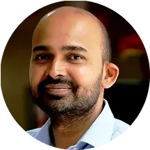
Professor. Ankur Gupta
Associate Professor
Centre for Applied Research in Electronics
Indian Institute of Technology Delhi
Prof. Ankur Gupta is an Associate Professor in the Centre for Applied Research in Electronics (CARE) at IIT Delhi. He is also a core member of the VLSI Design Tools and Technology (VDTT) programme offered jointly with the Electrical Engineering and Computer Science departments.
He holds a Master’s degree in VLSI & Embedded Systems and a Ph.D. in Microelectronics. With over 12 years of experience in VLSI and Microelectronics, he has also spent more than 6 years in the industry, working with top global companies including Intel Inc., Texas Instruments, and Global Foundries.

Professor Pushparaj Singh
Associate Professor
Microelectromechanical systems (MEMS) sensors and Microelectronics
Indian Institute of Technology Delhi
Prof. Pushpapraj Singh has received M. Tech. (Solid State Technology) from Indian Institute of Technology Madras, India in 2007. He moved to Nanyang Technological University (NTU) Singapore in January 2008 for his PhD under Prof. Miao Jianmin. In his PhD thesis work, he conducted extensive work for the piezoresistive sensitivity enhancement in silicon nanowires, planar and nanowire transistors. He also introduced the novel concept of gate-all-around junction less transistor as an improved sensing element for improving the strain detection limits.
After PhD, Dr. Singh has continued (since December 2011) his research work as a Research Scientist in A*STAR Institute of Microelectronics (IME), Singapore while working on several MEMS projects (MEMS based switches and non-volatile memories, piezoresistive and acoustic wave pressure/force sensors, inertial sensors, miniaturized medical devices). He joined CARE, IIT Delhi as an Assistant Professor in September 2016.

Professor Rahul Mishra
Assistant Professor
Nanoelectronics, spintronics, neuromorphic devices
Indian Institute Of Technology Delhi
Prof. Rahul received Ph.D. (Dec 2018) in Electrical and Computer Engineering from National University of Singapore, Singapore and B.Tech-M.Tech (Dual degree 2006-2011), in Electrical Engineering from Indian Institute of Technology, Kanpur, India.
He was a Postdoctoral Researcher (Dec 2018 – Sep 2020) at National University of Singapore, Singapore and a Graduate Student (Aug 2014 – Dec 2018), National University of Singapore, Singapore. He has industrial experience working as a Component Design Engineer in Intel Corporation, Bangalore, India from 2011-14.
Programme Sample Certificate
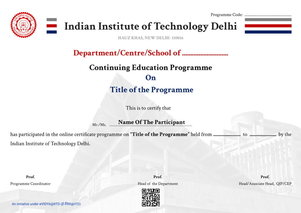
Participation Certificate: Candidates who maintain a minimum of 50% attendance will receive a Certificate of Participation from IIT Delhi's CEP.
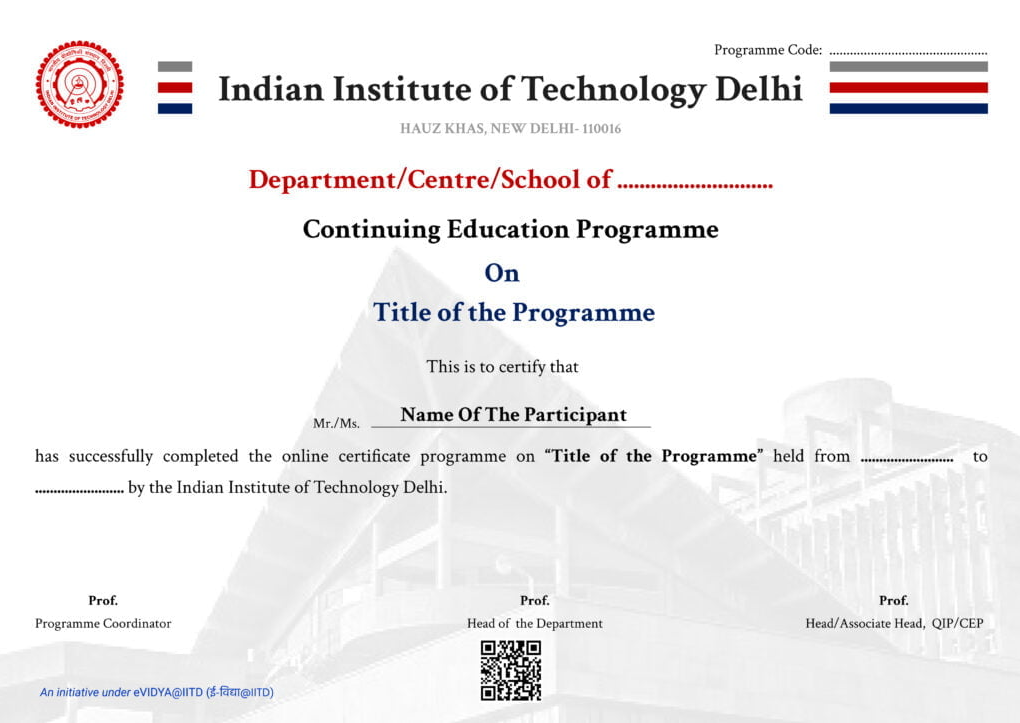
Completion Certificate: Candidates who score at least 60% marks overall and maintain a minimum of 50% attendance will be awarded a Certificate of Completion from IIT Delhi's CEP.
Only e-certificates will be issued by CEP IIT Delhi.
The organizing department of the programme is the Centre for Automotive Research and Technology, IIT Delhi.
Installment Schedule
Programme Fee INR 1,35,000 + GST
Instalment | Date | Amount (in ₹)** |
Application Fee* | To be paid at the time of application | 1,000 |
1st Instalment | Within one week of the offer rollout | 54,000 |
2nd Instalment | 30th July, 2026 | 54,000 |
3rd Instalment | 10th September, 2026 | 27,000 |
Note
*GST @ 18% will be charged extra in addition to the fees
**The application fee of ₹1000 plus 18% GST is non-refundable and non-transferable.
This fee is in addition to the programme fee and will not be adjusted against the total programme fee.
Refund Policy
Candidates can withdraw within 15 days from the programme start date. A total of 80% of the total fee received will be refunded. However, the applicable tax amount paid will not be refunded on the paid amount.
Candidates withdrawing after 15 days from the start of the programme session will not be eligible for any refund.
If you wish to withdraw from the programme, you must email cepaccounts@admin.iitd.ac.in and iitd-support@hclguvi.com stating your intent to withdraw. The refund, if applicable, will be processed within 30 working days from the date of receiving the withdrawal request.
Frequently asked questions
This programme is offered by the Continuing Education Programme (CEP), IIT Delhi.
It is a 6-month live online programme with live online sessions every Sunday from 10:00 AM to 1:00 PM IST.
Graduates or diploma holders from recognised institutions are eligible to apply. Preference may be given to candidates with relevant academic background or experience.
Selection is based on application review, academic background, and verification conducted by IIT Delhi Programme Coordinator. An interview may be required.
The total programme fee is ₹1,35,000 + 18 % GST. A ₹1,000 + 18 % GST non-refundable application fee is payable at the time of applying. The remaining fee can be paid in installments upon selection.
Yes. An 80% refund (excluding GST) is available if withdrawal is requested within 15 days of the first session.
Yes, recordings of live sessions will be available for participants throughout the programme duration.
Participants meeting the evaluation criteria will receive a Certificate of Completion from CEP, IIT Delhi. Those meeting minimum attendance requirements but not evaluation thresholds may receive a Participation Certificate. Only e-certificates are issued.
The programme covers the complete digital VLSI design flow including CMOS design, RTL development, synthesis, static timing analysis, design for testability, physical design, low-power methodologies, and advanced semiconductor technologies.
Yes, a three - day IIT Delhi campus immersion is included towards the end of the programme. Travel and accommodation cost will be borne by the participants. IIT Delhi is not responsible for the same.