
Executive Programme in Semiconductors, AI and Deep-Tech Entrepreneurship (Batch 2)
Features
Programme Overview
The semiconductor and photonics revolution is at the core of modern AI and high-performance computing (HPC), high-performance systems, and next-generation data centers. CEP IIT Delhi’s Executive Programme in Semiconductors, AI, and Deep-Tech Entrepreneurship is designed for professionals aiming to innovate at the intersection of advanced hardware technologies and entrepreneurship. Through 80 hours of live online learning, participants gain a strong understanding of semiconductor and photonic devices for AI and HPC, along with insights into commercialization, IP strategy, funding, and startup scaling—preparing them to build and lead deep-tech ventures.
₹ 1,50,000 + 18 % GST
Class Schedule
9:30 am - 12:30 pm, Sundays
Eligibility Criteria
Any Graduate
Programme Highlights
E-Certificate Of Successful Completion From CEP, IIT Delhi
Interdisciplinary Learning At The Cutting Edge
Deep-Tech Entrepreneurship Focus
Industry-Relevant Case Studies
Reputation & Recognition
2 -Day Campus Immersion
Programme Modules
Objective:
Build a foundational understanding of semiconductor physics and photonics, focusing on the technologies that drive modern computing and communication.
Semiconductor physics fundamentals, semiconductor diodes, BJTs, MOSFETs, and FinFETs
Current status and future perspectives of electronic integrated circuits
Electronics versus photonics: limitations and opportunities
Motivation for photonic integrated circuits (PICs)
PIC components: waveguides, resonators, couplers, optical modulators, and photodetectors
Current status and future trends of PIC technologies
Objective:
Understand the key semiconductor electronic devices used in AI accelerators, data centers, and high-performance computing systems.
Advanced CMOS, SOI, and FinFET Technologies
AI and Machine Learning Hardware: TPUs and GPUs
Neuromorphic and Memristor-based Devices: Brain-inspired computing for AI.
Objective:
Focus on the real-world applications of semiconductor photonic devices and photonics in modern AI, data centers, and computing.
Data Center Infrastructure: Photonic interconnects, co-packaged optics, optical switching, energy-efficient hardware, and scalable architectures.
Hardware Accelerators for AI Workloads: Machine learning models, photonic matrix processor, different neural network architectures (CNN, RNN, DNN, etc.), real-world applications of neural networks for signal processing and image processing.
Objective:
Bridge the gap between technical innovations and commercialization, with a focus on launching semiconductor or photonics-based startups. Learn how to transform your technical innovation into a market-ready product and scale it successfully.
From Lab to Market: Prototyping, manufacturing partnerships, and productization.
Overview of Deep-Tech Entrepreneurship: Ecosystem, challenges, and opportunities in hardware startups.
Technology Readiness Levels (TRL): Moving from basic research to product development.
Commercialization Models for Hardware: Fabless, semiconductor foundry partnerships, system-level integration.
Intellectual Property (IP) Strategy: Patents, licensing, and tech transfer in semiconductor and photonics.
Funding Deep-Tech Startups: Sources of funding (VC, government grants, angel investors, corporate R&D partnerships).
Scaling Semiconductor Startups: Production scaling, supply chain management, and cost optimization.
Go-to-Market Strategies: Market fit, pricing, distribution, and competitive differentiation.
Building and Leading Teams: Effective leadership and talent acquisition for deep-tech companies.
Objective:
Analyze real-world examples and engage with industry experts to understand how semiconductor innovations are commercialized.
Case Study 1: TPU and AI hardware development
Case Study 2: Photonic AI accelerators
Case Study 3: Optical interconnects for data centers
Case Study 4: Global semiconductor ecosystem
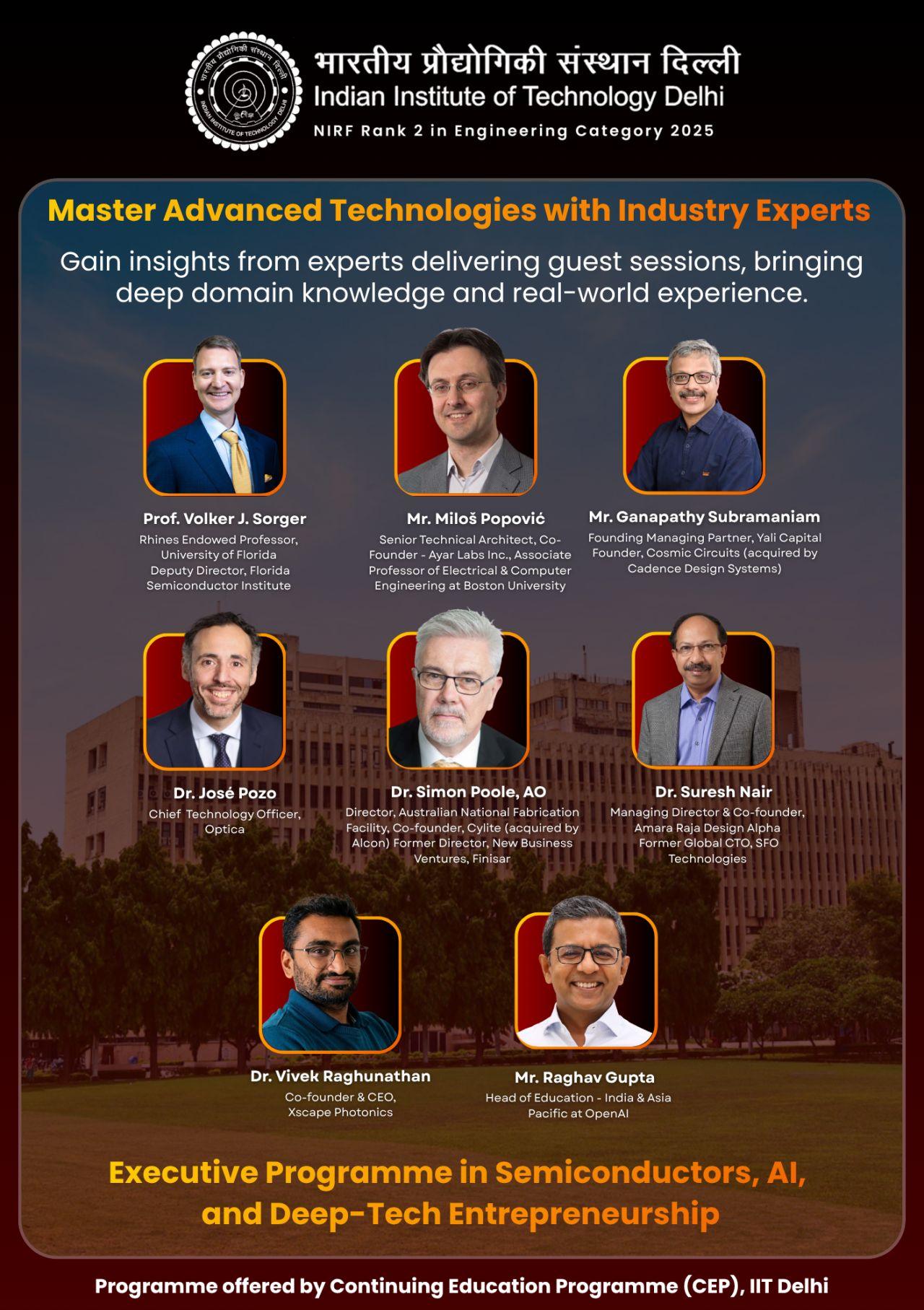
Guest Lectures and Panel Discussions: Startup founders, VCs, and industry experts
All case studies are based on publicly available information and independent academic analysis.
Objective:
Equip participants with the skills to pitch their ideas to investors, raise funds, and grow their deep-tech ventures.
Pitch Deck Creation: Building a compelling pitch for investors
Investor Expectations: What VCs and angel investors look for in semiconductor/photonics startups
Funding Strategy: Choosing the right funding path for your startup (VC, angel investors, government grants)
Mock Pitch Sessions: Practice pitching ideas to mock investors for feedback.
Learning Outcomes
Semiconductor & Photonic Foundations:
Develop a strong understanding of semiconductor physics and photonics fundamentals, including band structure, carrier transport, light–matter interaction, and core device technologies.
Advanced Devices for AI & HPC:
Understand advanced CMOS, FinFETs, neuromorphic devices, memristors, and next-generation transistors, along with AI and machine learning hardware such as GPUs, TPUs, and photonic matrix processors.
Photonics for Modern Computing:
Gain insights into photonic integrated circuits, optical interconnects, co-packaged optics, and photonic chips used in AI, data centers, and computing systems.
Commercialization & IP Strategy:
Learn how to transition from research to product, covering Technology Readiness Levels (TRL), patenting strategies, licensing, and technology transfer in semiconductor and photonics domains.
Deep-Tech Startup Scaling:
Acquire practical knowledge of funding models, manufacturing partnerships, supply chain considerations, go-to-market strategies, and leadership challenges in scaling hardware-focused startups.
Pitching & Fundraising Skills:
Build investor-ready pitch decks, understand VC and angel investor expectations, and practice pitching through mock investor sessions.
Programme Coordinator
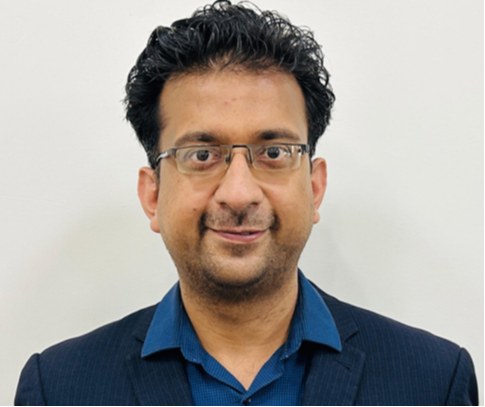
Professor Deepak Jain
Associate Professor
Optics & Photonics Center
Indian Institute of Technology Delhi
Deepak Jain is an Associate Professor at the Optics & Photonics Center, IIT Delhi, and a deep-tech entrepreneur. He previously served as faculty in the Electrical Engineering Department at IIT Bombay and held prestigious research fellowships at the University of Sydney and the Technical University of Denmark. He earned his Ph.D. from the Optoelectronics Research Centre, University of Southampton, UK. Prof. Jain’s work lies at the intersection of semiconductors, photonics, artificial intelligence, and scalable deep-tech systems. His contributions span semiconductor diode lasers and beam-shaping fibers, high-power and specialty fiber lasers, hollow-core optical fibers, and photonic matrix processors for AI acceleration. He is leading India’s first national Department of Telecommunications (DoT)-supported project on hollow-core fibers for next-generation data centers and quantum communication. He has taught advanced courses on Semiconductor Devices & Circuits, Semiconductor Special Devices (optoelectronics), Integrated Photonics, and Photonics Matrix Processors for AI. He has authored over 60 publications, holds more than 10 patents, raised over ₹15 crore for research at IIT Delhi, and over ₹30 crore for startup initiatives. Prof. Jain is the founder of Deeplase Technologies, focused on lasers, hollow-core fibers, and photonic AI hardware. A TEDx speaker, and Senior Member of Optica and IEEE, his executive teaching emphasizes how deep-tech innovations are built, funded, and scaled from lab to market.
Programme Faculty
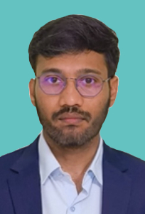
Professor A. Aadhi
Assistant Professor
Optics & Photonics Center
Indian Institute of Technology Delhi
Prof. A. Aadhi is currently an Assistant Professor at the Optics and Photonics Centre, Indian Institute of Technology Delhi. His research expertise includes photonic computing, neuromorphic photonic processors, integrated photonics, nonlinear optics, and the generation of structured light beams.
He earned his PhD in 2016 from IIT Gandhinagar and the Physical Research Laboratory. He is also currently a visiting scientist at Queen’s University, Canada. From 2017 to 2025, he was a postdoctoral researcher at several leading institutes, including the Institute National de la Recherche Scient fique (INRS), Canada; Queen’s University, Canada; and the Singapore University of Technology and Design (SUTD), Singapore.
He has published more than 50 research articles in high-impact journals such as Nature, Nature Communications, Optica, Advanced Science, Laser & Photonics Reviews, and Optics Letters, as well as more than 50 conference proceedings. Prof. Aadhi holds six international patents and several Editor’s Pick articles in leading journals. He has received several national and international awards, fellowships, and has delivered numerous invited talks at major international optics and photonics conferences, including CLEO, SPIE, IEEE, Euro photonics, and Photonics North.
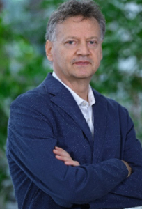
Professor Mihai Sanduleanu
Associate Professor
Electrical Engineering, Khalifa University, UAE
Received his MSc, MEE and PhD degrees from the Technical University of Iasi, Romania, Eindhoven University of Technology, The Netherlands and University of Twente, The Netherlands in 1990, 1993 and 1999, respectively. From 1999 to 2000, he was with Philips Semiconductors, Nijmegen, The Netherlands, working on fiber optic communication circuits. From 2000 to 2007 he joined Philips Research Eindhoven, The Netherlands and he was involved in Fiber Optic Interface circuits, RF IC Design, mm-Waves Transceiver design and Ultra-low-power radios. From 2008 to 2013, he conducted research at IBM T.J. Watson Research Center, Yorktown Heights, New York in mm-Waves transceivers for communication, imaging and RADAR, THz electronics.
He is currently Associate Professor at Khalifa University of Science and Technology. Dr. Sanduleanu’s area of expertise include Wireless transceiver design for RF/mm-Waves/THz communication, High Speed Communication Circuits for serial I/O, High speed analog-to-digital converters, Phased-Array Systems, High-speed digital circuits and systems. Dr. Sanduleanu authored/co-authored 9 books and more than 140 papers in International Conferences and Journals. He holds 54 US patents. Dr. Sanduleanu served as Associate Editor for IEEE Transactions on Circuits and Systems in 2011–2012 and he is Associate Editor for Springer Nature “Analog Integrated Circuits and Signal Processing”.
Programme Sample Certificate
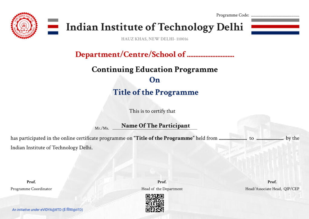
Participation Certificate: Awarded to those with at least 40% attendance.
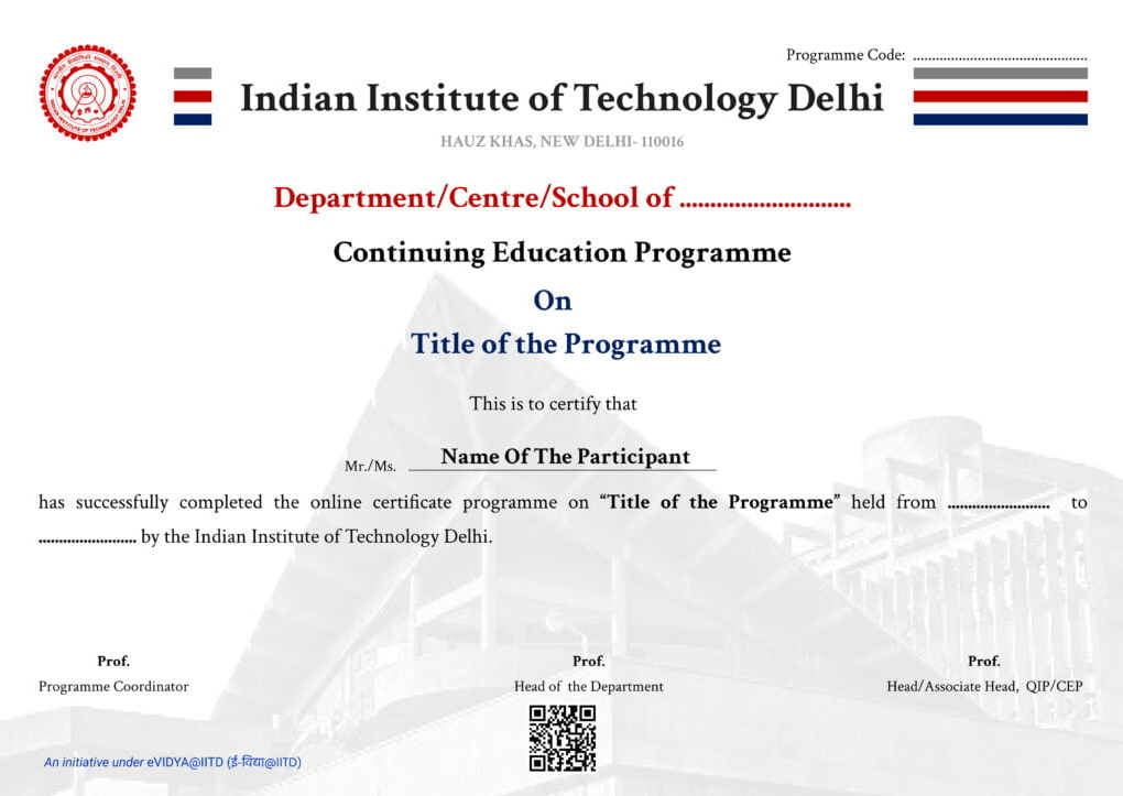
Successful Completion Certificate: Awarded to those with at least 40% attendance and a minimum of 50% marks.
Notes
The above e-certificate is for illustrative purposes only and the format of the e-certificate may be changed at the discretion of IIT Delhi.
Only e-certificate will be provided and it will be issued by CEP, IIT Delhi.
The organizing department of this programme is the Optics & Photonics Center, IIT Delhi.
Installment Schedule
Programme Fees: 1,50,000 + 18 % GST
Installment | Installment Date | Amount (₹) |
I | Within 3 Days of the offer letter. | ₹ 75,000+ 18 % GST |
II | 9th January, 2027. | ₹ 75,000+ 18 % GST |
Note:
*All fees should be submitted in the IITD CEP account only, and the details will be shared post-selection.
*The receipt will be issued by the IIT Delhi CEP Account for your records, which can be downloaded from the CEP Portal.
*GST @ 18% will be charged extra in addition to the fee.
Refund Policy
Candidates can withdraw within 15 days from the programme start date. A total of 80% of the total fee received will be refunded. However, the applicable tax amount paid will not be refunded on the paid amount.
Candidates withdrawing after 15 days from the start of the programme session will not be eligible for any refund.
If you wish to withdraw from the programme, you must email cepaccounts@admin.iitd.ac.in and cepdelhi@digiversity.com, stating your intent to withdraw. The refund, if applicable, will be processed within 30 working days from the date of receiving the withdrawal request.
Frequently asked questions
The Executive Programme in Semiconductors, AI, and Deep-Tech Entrepreneurship is a structured executive education programme designed to provide professionals with an integrated understanding of semiconductor technologies, advanced device architectures, and deep-tech venture creation. The programme covers semiconductor fundamentals, emerging electronic and photonic device concepts, and the entrepreneurial frameworks required to translate deep-tech innovations into scalable ventures, delivered through live online sessions and applied learning.
Unlike standalone semiconductor or technology-specific courses, this executive programme adopts a cross-disciplinary approach, combining semiconductor technologies, photonic systems, and deep-tech entrepreneurship within a single curriculum. It enables participants to understand not only how advanced technologies are developed, but also how they can be commercialized, scaled, and positioned within the deep-tech ecosystem, under academic guidance from IIT Delhi.
This programme is suitable for working professionals, engineers, technologists, researchers, startup founders, and aspiring entrepreneurs who are interested in semiconductors, photonics, and deep-tech innovation. It is particularly relevant for individuals involved in electronics, device engineering, product development, R&D, technology strategy, or those looking to build or scale deep-tech ventures.
Prior hands-on experience in semiconductors or photonics is not mandatory. However, a basic background in engineering, technology, or applied sciences is beneficial. The programme introduces core concepts in a structured manner, making it suitable for professionals transitioning into semiconductor and photonic device domains or seeking to broaden their existing technical and entrepreneurial skill set.
The programme includes a two-day on-campus immersion at IIT Delhi, offering participants the opportunity to engage directly with faculty and peers. However, travel, accommodation, and other related expenses are not included in the programme fee and are to be borne by the participants.
Yes. The programme encourages interaction through live online sessions, discussions, and applied learning activities, allowing participants to engage with IIT Delhi faculty and peers. Additionally, the on-campus immersion provides valuable face-to-face interaction, fostering peer learning, collaboration, and professional networking within the semiconductor and deep-tech ecosystem.