
Online Post Graduate Diploma in VLSI Design
Features
Programme Overview
Very Large Scale Integration (VLSI) Design is a cornerstone of modern electronics, enabling the creation of complex integrated circuits that power everything from smartphone and computers to medical devices and automotive systems. As technology continues to advance toward higher performance, lower power consumption, and smaller form factors, the demand for skilled VLSI design experts has grown exponentially. A VLSI design programme equips students and professionals with the knowledge and practical skills required to design, analyze, and optimize semiconductor devices and VLSI circuits and systems. Through a blend of theoretical foundations, hands on laboratory, experience, and exposure to industry standard tools, the programme prepares learners to contribute to cutting edge innovations in chip design, electronic system development, and next generation hardware technologies. IIT Delhi's Online PG Diploma in VLSI Design is your opportunity to master the art of VLSI Design and contribute to the growth of semiconductor industry, nation and mankind.
Whether you are an engineering student, working professional or a VLSI enthusiast, this programme provides the skills and confidence to excel in Semiconductor and VLSI Design.
₹ 3,50,000 (Including GST)
Affiliate Alumni Benefits
Benefits: The Affiliate Alumni, with prior approval from the Alumni and Endowment Office, are allowed to visit the IIT Delhi campus as per the Institute visitor’s policy.
Class Schedule
Saturday & Sunday
10:00 AM to 12:30 PM (IST)
02:00 PM to 05:30 PM (IST)
Eligibility Criteria
Graduates, Postgraduates and working professionals with B.E./B.Tech. in Electrical Engineering, Electronics Engineering or equivalent in related areas and M.sc (Physics/Electronics)
Programme Highlights
12 -Month Structured Learning
30 -credit IIT Delhi Online PG Diploma
Live Sessions By IIT Delhi Faculty
Campus Immersion* (Optional)
Affiliate Alumni Status From IIT Delhi
Weekend-only Format
Programme Modules
Course 01: Fundamental Circuit Analysis (3 Credit)
Network analysis techniques, network theorems, transient and steady state analysis, Network graphs, two port networks, transmission lines, scattering matrix, network synthesis, Butterworth and Chebyshev approximations, Active and passive filter Design
Learning Outcome
To perform circuit analysis, and analyze time domain and frequency domain behavior of circuits.
To design and analyze different filters and its circuits
Course 02: Digital Electronics (3 Credit)
Number systems, combinational and sequential circuits, Asynchronous, synchronous counters. Finite state machines, Mealy, Moore machines. Static timing analysis, Memories. Introduction to logic families, Static and dynamic logic, HDL language (Verilog).
Learning Outcome
To understand the fundamental principles of digital systems, Analyze and design basic digital circuits using combinational and sequential logic.
Apply digital electronics concepts to real-world applications by constructing and testing digital circuits using hardware and simulation tools.
Course 03: Fundamentals of Analog circuit design (3 Credit)
Small signal analysis, negative feedback, introduction to MOSFETs, biasing circuits, single stage amplifiers, frequency analysis of single stage amplifiers, differential amplifiers, frequency compensation and two-stage OTA.
Learning Outcome
To understand the fundamentals of analog circuit design.
To design basic analog circuits such as amplifiers, current mirrors and biasing circuits.
To get an exposure of use of analog circuits in real life application.
Course 04: MOS VLSI (3 Credit)
CMOS process, scaling, yield and reliability, static CMOS combinational logic physical design and optimization, static CMOS/MOS sequential logic physical design and optimization, other CMOS logic families, clock domain crossing, static and dynamic power analysis, Memories.
Learning Outcome
Understand digital combinational logic design structures and optimization methods using various MOS and CMOS logic families.
Delay models and their effects on circuit performance.
Power and area optimization techniques.
Course 05: Mini Project (3 Credit)
A live project on advanced circuit design.
Learning Outcome
Will be able to design and analyze circuits for real-world problems.
Course 06: Advanced Analog Design (3 Credit)
Basics of IC design, negative feedback, frequency compensation, noise analysis, slew and mismatch in op-amp, biasing scheme, single-stage operational amplifier and its frequency analysis, multi-stage op-amps, voltage and current references, basics of switched capacitor circuit, filters, oscillators.
Learning Outcome
To understand the fundamentals of analog IC design.
To gain an expertise of different analog circuits required for design and to get an exposure of use of analog circuits in real life problems.
Course 07: Mixed Signal Circuit Design (3 Credits)
Switched capacitor circuit principles and applications in filter design, design and analysis of switches, sample and hold circuits, data converters: static and dynamic characteristics, comparators, classification. Flash, pipeline, SAR ADCs, discrete-time and continuous-time delta-sigma ADCs, introduction to DACs and its design.
Learning Outcome
In-depth knowledge on design and characterization of mixed signal circuit blocks such as switched capacitor based filters, digital to analog converters (DACs) and analog to digital converters (ADCs).
Course 08: IEC Lab (3 Credits)
Introduction to CMOS design flow, schematic design and simulation, DC and AC analysis, noise analysis, stability analysis, layout design, DRC, LVS and parasitic extraction, simulation of parasitic extracted netlist.
Learning Outcome
Understand the use of VLSI Design tools for layout design and verification (DRC), circuit simulation, estimation of area, timing, and power.
Design of standard cells, elementary understanding of hierarchical design using tools.
Design of a medium complexity VLSI block to meet prescribed area, timing and power specifications.
Course 09: Major Project (6 Credits)
This project provides learners with the opportunity to apply the concepts learned in previous courses for development of integrated electronics, circuits and systems. Identify a real-world problem, design a circuit, system or algorithmic solution, and validate it through industry relevant simulation tools and experimentation.
Learning Outcome
Design, analyze and solve a problem in the area of integrated electronics, circuits and systems.
Effectively communicate technical findings through written and oral formats, demonstrating critical thinking and the ability to reflect on the broader impact of integrated electronics, circuits and systems related technologies.
NOTE: The sessions will be delivered by IIT Delhi faculty and Industry Experts brought by the Programme coordinator only.
Kindly Note: Curriculum is subject to change and modification as per the requirement of the programme. IIT Delhi and Programme Coordinator’s decision will be final.
DISCLAIMER:
Online PG Diplomas are the academic programme of IIT Delhi, and there is no campus placement or assistance provided from IIT Delhi in these programmes. The evaluation of minor and major projects is subject to the faculty’s discretion, based on academic guidelines and instructional objectives. Assessment criteria may vary depending on the nature of the project and its alignment with the course framework.
Learning Outcomes
Design end-to-end VLSI circuits
across analog, digital and mixed-signal systemsUnderstand the full CMOS design flow
from schematic to layoutBuild a real project portfolio
through hands-on labs, mini and major projects on industry toolsStep into advanced VLSI roles
across India's growing chip design ecosystem
Programme Coordinator
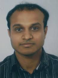
Professor Mukul Sarkar
Professor
Department of Electrical Engineering
Indian Institute of Technology Delhi
Expertise
CMOS Image Sensors
Analog/Digital Circuit Design
Bio-inspired Vision
Optoelectronics
About the faculty
A specialist in CMOS image sensors and bio-inspired vision.
Has been shaping analog and mixed-signal research at IIT Delhi since 2012.
Works across CMOS image sensors, optoelectronics and analog/digital circuit design.
Holds a PhD from TU Delft, Netherlands.
Former full-time resident at IMEC.

Professor Ankesh Jain
Associate Professor
Department of Electrical Engineering
Indian Institute of Technology Delhi
Expertise
Analog & Mixed-Signal Circuits
Data Converters
On-chip Power Management
About the faculty
A former semiconductor industry engineer with expertise in analog and mixed-signal circuits.
Leads research and teaching in analog and mixed-signal design and data converters at IIT Delhi.
Works across data converters, on-chip power management and integrated circuit design.
Holds a PhD from IIT Madras.
Formerly associated with Freescale Semiconductor and serves as Associate Editor, IEEE Transactions on Circuits and Systems II.
Programme Faculty
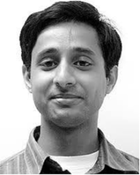
Professor Shouri Chatterjee
Professor
Department of Electrical Engineering
Indian Institute of Technology Delhi
Expertise
Mixed-Signal & Analog IC Design
Filter Design
Ultra-Low-Power Circuits
About the faculty
An integrated circuit design expert with work spanning filters and analog IC design.
Researches ultra-low-power circuits for energy harvesting and mm-wave radio front ends.
Brings expertise across mixed-signal design, analog circuits and filter design.
Holds a PhD from Columbia University.
Formerly associated with Silicon Laboratories, USA, and is a Senior Member, IEEE.
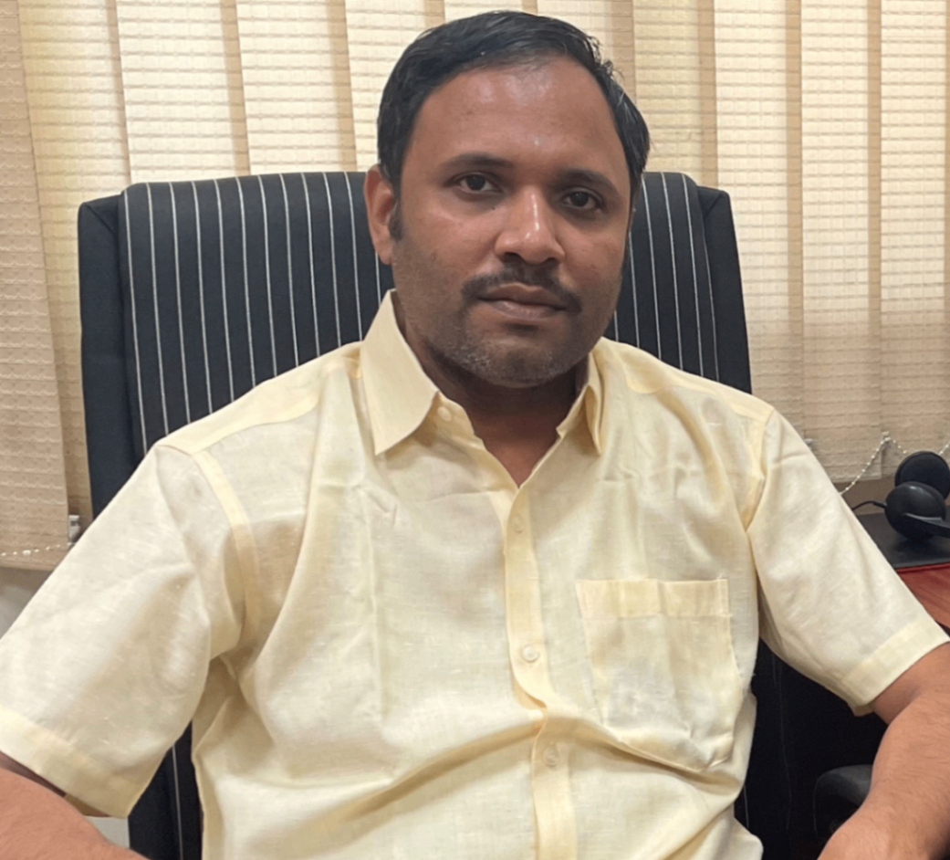
Professor Rakesh K. Palani
Associate Professor
Department of Electrical Engineering
Indian Institute of Technology Delhi
Expertise
Analog & Mixed-Signal Circuits
Data Converters
Op-Amp Design
About the faculty
Leader of IIT Delhi's Mixed Signal Group.
Designs op-amps, ADCs and DACs with a strong focus on high-performance analog and mixed-signal systems.
Brings years of high-performance semiconductor industry design experience.
Holds a PhD from the University of Minnesota.
Formerly associated with Broadcom, Maxlinear and Qualcomm, and serves as Chair, IEEE Delhi Section CAS-CSS.

Professor Mustafijur Rahman
Assistant Professor
Department of Electrical Engineering
Indian Institute of Technology Delhi
Expertise
CMOS RF/mm-Wave IC Design
Transceiver Architectures
Cryogenic ICs
About the faculty
A former Intel Labs research scientist working on next-generation CMOS transceivers.
Researches IC technologies for 6G, automotive RADAR and quantum computing hardware.
Works across CMOS RF/mm-wave IC design, transceiver architectures and cryogenic ICs.
Holds a PhD from the University of Minnesota.
Formerly associated with Intel Labs and Qualcomm Atheros, and received the Teaching Excellence Award 2023 at IIT Delhi.

Professor Dhiman Mallick
Associate Professor
Department of Electrical Engineering
Indian Institute of Technology Delhi
Expertise
MEMS/NEMS
Energy Harvesting
Piezoelectric & Magnetoelectric Sensors
About the faculty
Head of the Interdisciplinary Microsystems Lab.
Researches MEMS, energy harvesting and smart sensors for autonomous and IoT systems.
Works across MEMS/NEMS, piezoelectric sensors and magnetoelectric sensor systems.
Holds a PhD from Tyndall National Institute, Ireland.
DST INSPIRE Faculty Awardee and Member, IEEE.
Programme Sample Certificate
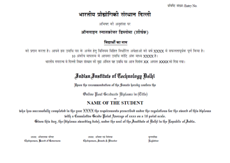
The above Online PG Diploma is for illustrative purpose only, and the format of the certificate may be changed at the discretion of IIT Delhi.
The organizing department for this Online PG Diploma is the Department of Electrical Engineering
Installment Schedule
Programme Fees: ₹ 3,50,000 (Including GST)
Component | Date | Amount (in ₹)* |
Application Fee* | To be paid at the time of Application | 1,000/ + 18 % GST |
1st Instalment | To be paid within 7 days of Offer release | 50,000/- (Including GST) |
2nd Instalment | 28th Jan 2027 | 50,000/- (Including GST) |
3rd Instalment | 22nd Feb 2027 | 85,000/- (Including GST) |
4th Instalment | 22nd Mar 2027 | 85,000/- (Including GST) |
5th Instalment | 22nd April 2027 | 80,000/- (Including GST) |
Affiliate Alumni Membership Fee* | Payable separately, immediately before the 2nd instalment. Affiliate Alumni benefits will be available upon programme completion. | 10,000/- +GST |
Re-examination fee (per course, per attempt) ₹10,000/- + GST | ||
Note:
Programme Fee: GST is included. The application fee and affiliate alumni fee are not a part of the total programme fee.
Re-examination Fee: Re-examination Fee: Re-examination is permitted for up to three attempts within three years of programme completion, subject to a fee of ₹10,000 + GST per course per attempt.
Affiliate Alumni Status: To secure the Affiliate Alumni Status, learners will have to pay a one-time, non-refundable, mandatory affiliate alumni membership fee of ₹10,000 + taxes at the time of admission, which is over and above the Programme Fee.
Refund Policy
All fees paid are non-refundable and non-transferable.
Frequently asked questions
The semiconductor industry is entering its most transformative decade. From AI accelerators and 5G/6G to electric vehicles, IoT and consumer electronics, every breakthrough in technology is powered by a chip designed by a VLSI engineer.
As India scales its semiconductor mission with new fabs, design centres and a widening talent gap, organisations need professionals with deep, end-to-end expertise in chip design. Building expertise in VLSI enables professionals to contribute across analog, digital, mixed-signal design, verification, layout and system integration.
Depending on their experience, technical background and existing function, professionals can explore roles such as:
VLSI Design Engineer
Analog Design Engineer
Digital Design Engineer
Mixed-Signal Design Engineer
ASIC Design Engineer
RTL Design Engineer
Physical Design Engineer
Verification Engineer
CMOS Layout Engineer
Semiconductor R&D Engineer
Embedded Hardware Engineer
FPGA Design Engineer
Career relevance will vary based on the participant's prior experience, technical expertise and organisational requirements.
It is a 12-month programme offered through the Continuing Education Programme (CEP), IIT Delhi, with the Department of Electrical Engineering as the organising department.
The programme covers the full VLSI design stack, including circuit fundamentals, digital electronics, analog and advanced analog design, MOS VLSI, mixed-signal circuit design, and the complete CMOS design flow through applied lab work and projects.
The programme combines:
LIVE interactive learning from IIT Delhi faculty
A curriculum spanning the full VLSI design stack
Hands-on IEC Lab work on industry-standard tools
Mini and major design projects
A 2 day optional campus immersion at IIT Delhi
Online Post Graduate Diploma from IIT Delhi
Affiliate Alumni Status of IIT Delhi
The programme is designed for:
Working professionals in electronics, embedded systems or hardware roles looking to build deep VLSI expertise
Engineers and engineering managers preparing to move into advanced VLSI design roles
Academicians and researchers looking to build practical, hands-on chip design expertise